Floating-gate transistors based on two-dimensional semiconductors offer a promising platform for compact memory devices, yet the role of lateral device geometry in determining their hysteretic characteristics remains insufficiently understood[1,2]. Here, we investigate MoS2 floating-gate transistors with systematically varied device dimensions and introduce a geometric area ratio (𝑅𝐴 = 𝐴CH−FG/𝐴G−FG) to quantify the relative overlap geometry between the channel, floating gate, and control gate (Fig. 1a). The memory window (MW) increases strongly with increasing 𝑅𝐴,demonstrating pronounced geometrydependent modulation of the memory response (Fig. 1b), while the increase becomes progressively weaker at large 𝑅𝐴 (Fig. 1c). Sweep-rate measurements further show that the MW is enhanced at slower gate sweeps, with the magnitude of this dependence varying with 𝑅𝐴, indicating an interplay between device geometry and finite charge-transfer dynamics (Fig. 1d). Measurements across 60 devices under the same geometry and measurement conditions further demonstrate good device-to-device reproducibility (Fig.1e). Transient TCAD simulations incorporating Fowler–Nordheim tunneling further show that changing 𝑅𝐴 substantially modifies the evolution of floating-gate charge during gate sweeps, consistent with the experimentally observed hysteresis modulation (Fig. 1f). The correspondence between the simulated Δ𝑄FG evolution and the measured MW supports floating-gate charge modulation as an underlying physical mechanism for the geometry-dependent memory behavior. These results establish lateral geometry as an effective design parameter for tuning floating-gate memory characteristics and provide a physical link between device dimensions, floating-gate charge dynamics, and electrical hysteresis.
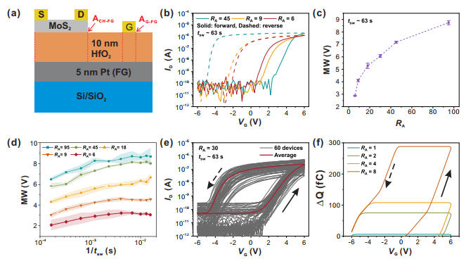
Figure 1: Geometry-dependent memory behavior in MoS2 floating-gate transistors. (a) Device schematic and definition of the geometric area ratio 𝑅𝐴 = 𝐴CH−FG/𝐴G−FG, where 𝐴CH−FG and 𝐴G−FG denote the channel–floatinggate and gate–floating-gate overlap areas, respectively. (b) Representative dual-sweep 𝐼𝐷–𝑉𝐺 characteristics for different 𝑅𝐴. (c) Extracted MW versus 𝑅𝐴. (d) Frequency dependence of the MW for representative 𝑅𝐴 values. (e)𝐼𝐷–𝑉𝐺 characteristics of 60 devices measured under the same condition. (f) TCAD-simulated floating-gate charge variation Δ𝑄FG for different 𝑅𝐴, showing geometry-dependent charge evolution.
[1] Y. Cai et al., Nature Communications 16, 2649 (2025). [2] Y. Wang et al., Nature Communications 16, 9268 (2025).